
AttoMap-200
XRF Microscope
Highest resolution on the market
Large stage travel and enclosure

Key Advantages:
- Highest resolution laboratory microXRF
Achieve down to single digit microns (3-5 µm) with high resolution optic - Sub-ppm sensitivity
Quantify down to sub parts per million (ppm) levels with Sigray’s flexible software packages - Energy tunability
Maximize throughput and sensitivity with up to 5 different incident x-ray spectra - Large Travel and Enclosure
Enables unsupervised overnight scans. Also provides opportunity to integrate correlative techniques such as Raman Spectroscopy
Highest Resolution of any XRF Microscope on the Market
Micro x-ray fluorescence (microXRF) is a highly sensitive technique for compositional analysis, with sensitivities typically 1,000 times greater than those of electron-based spectroscopy (ppm vs. ppt). The primary limitation of laboratory-based microXRF has been the achievable spot sizes, which are typically around 20-50 µm. Sigray’s AttoMap achieves the highest spatial resolutions available—on the order of single digit micrometers (3-5 µm)—through the use of Sigray’s proprietary x-ray focusing optics. These optics are significantly more efficient and produce far smaller spot sizes than the polycapillary optics used in other laboratory microXRFs systems.

Sub-ppm Sensitivities (Sub-Femtogram)
AttoMap achieves unprecedented sensitivities, with absolute detection limits in the sub-femtogram range and relative detection limits below parts per million. This enables high-throughput microscopy of trace element distributions. The system’s accuracy and speed are why leading semiconductor companies have adopted the AttoMap for monitoring processes involving trace-level dopants.

Energy Tunability for High Throughput and Sensitivities
X-ray fluorescence is highly dependent on the energy of the illuminating x-ray beam. Fluorescence cross-sections can vary by several orders of magnitude, as shown in the corresponding table of a select number of elements. Sigray’s AttoMap-200 provides easy software-selection of up to five target materials, including exotic target materials such as a silicon-based source and a gold-based source, ensuring optimal sensitivity for a broad range of elements. In contrast, other x-ray sources are limited to only a single x-ray target material, which maximizes sensitivity and throughput for a subset of elements.
A visual representation of the impact of energy tunability through x-ray source target selection is shown in the image below, comparing an arsenopyrite sample imaged using a tungsten (W) target and a molybdenum (Mo) target.


Large Travel Range and Enclosure
AttoMap-200’s robust, heavy-duty stage can accommodate large samples or multiple samples (for automated overnight scanning). Samples include 300mm wafers and large rock core samples. The space inside the enclosure also permits modifications and upgrades, such as the integration of Raman Spectroscopy.
System Features
- Patented high brightness x-ray source with 50X brightness over those used in other leading microXRF systems and provides up to 5 different spectra in a single source
- Mirror Lens x-ray optics with major advantages over conventional polycapillary microXRF systems
- Wide range of flexible and intuitive software routines, from mineralogy to semiconductor-focused wafer pattern navigation, flexible and customizable Jupyter notebooks, and fundamental parameters analysis for weight percentages
Patented Multi-Target Ultrahigh Brightness X-ray Source
Sigray’s x-ray source, when combined with x-ray optics, provides over 50 times the brightness of the illumination beam (source + optics) systems used by other leading microXRF systems. This is achieved through a patented design in which multiple target materials are in optimal thermal contact with diamond, which has excellent thermal conductivity. The rapid cooling of diamond enables higher power loading on the x-ray source, producing an intense beams of x-rays. This thermal benefit allows for a greater variety of materials to be used as x-ray source target materials, each generating strong characteristic x-rays of a specific energy. Up to four target materials can be customized for the AttoMap-200 source, enabling software selection of the optimal spectra for your sample. The power of energy tunability is clearly demonstrated in the example shown previously.

Mirror Lens: Double Paraboloidal X-ray Optics
The focusing x-ray optic is as crucial as the x-ray source in determining the performance of any microXRF system. Sigray is the leading producer of x-ray optics and only manufacturer capable of fabricating the mirror lens x-ray imaging optics used in the AttoMap systems. Other microXRF systems use polycapillary optics to guide x-rays onto a spot on the sample.
Sigray’s mirror-lens optics overcome several major drawbacks of polycapillary optics, including their limited depth-of-field and chromatic aberrations. AttoMap’s larger depth-of-field enables high-resolution imaging of samples that cannot be finely polished to a flat surface and/or have topographical features. The absence of chromatic aberrations also allows for superior quantification, as there is only a single focal spot producing x-rays on the sample. In contrast, when chromatic aberration is present, different x-ray energies are focused to different diameters on the sample, making it challenging to determine the precise location of x-ray production.

Software
AttoMap-200 comes with a suite of extendable and intuitive software. The software provides different advantages, depending on the application of interest:
- Semiconductor: Automated pattern recognition on wafers enables high throughput recipe-based point analysis on wafers.
- Geology: Mineralogical classification through an AI-based clustering algorithm to segment grains and identify their mineralogy based on the elemental composition.
- Materials Science and Life Sciences: Weight percentage through both standards-based and standardless fundamental parameters analysis through a GUI interface. Sigray also provides Jupyter notebooks customized for quantification routines of interest and can be easily extended or modified by users with some understanding of Python.
Software functions include: Single and multi-file analysis, spectral fitting and deconvolution, fundamental parameter (FP) model implementation for standard-less quantification, relative weight percentage calculations using the FP model, spectral clustering using machine learning, spectral decompositions, optical and fluorescence image overlay, and open-box extensibility.

Applications
Mineralogy
Automated mineralogy using scanning electron microscope (SEM) has become a dominant approach in natural resource exploration and process monitoring. AttoMap provides a powerful complement to SEM-based mineralogy by offering 1000X the sensitivity of SEM-EDS for trace elemental mapping. The system’s intuitive software features AI-based grain segmentation and mineralogical identification.

Life Sciences and Metallomics
AttoMap was originally designed for life science research with support of NIH funding. Applications in the life sciences include studying pathologies (e.g., cancer and Wilson’s Disease) that are hypothesized to be related to the dysregulation of trace elements such as iron and copper, analyzing the distribution of nanoparticle-based therapeutics after injection, and examining the environmental uptake of contaminants.

Semiconductor
AttoMap has been adopted by leading semiconductor companies for monitoring dopants and ultrathin films on test patterns. The system also provides trace-level measurements of organic contaminants and low atomic number (Z) materials, such as boron (B), within its vacuum environment. Pattern recognition-based software enables unsupervised, recipe-based acquisition of points for high efficiency.
For backend packaging, AttoMap offers high throughput metrology of micropillar dimensions, quantification of voids in microbumps, and rapid identification of defects.

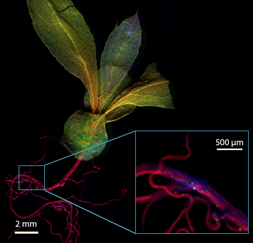
Environmental / Botany
Synchrotron XRF has become a technique of choice for many plant scientists studying element distribution. Such studies include metal uptake for phytoremediation (reclaiming the environment), nutrient absorption, and the development of genetically modified plants with desirable characteristics, such as drought resistance and improved nutritional content.
Technical Specifications of the AttoMap-200
| Parameter | Specification | |
|---|---|---|
| Overall | Spatial Resolution | Down to 3-5 μm with high resolution optic. 7-10 μm with standard optics. |
| Sensitivity | Sub-ppm relative detection sensitivity. Picogram to femtogram absolute sensitivity. | |
| Source | Type | Sigray patented ultrahigh brightness sealed microfocus source |
| Target(s) | Up to 5 targets. Includes selection from Si, Cr, Cu, Rh, W, Mo, Au, Ti, Ag. Others available upon request. |
|
| Power | Voltage | 50W | 20-50 kVp | |
| X-ray Optic | Type | Sigray proprietary double paraboloidal x-ray mirror lens |
| Transmission Efficiency | ~80% | |
| Magnification | 1:1 magnification default Optional demagnifying optics for higher resolution |
|
| Interior Coating | Platinum for increasing collection efficiency of optic | |
| X-ray Detector | Type | SDD Detector |
| Energy Resolution | <129 eV at Mn-Ka | |
| Dimensions | Footprint | 54" W x 65.5" H x 38.5" D |
| Stage Travel | 200 mm x 200 mm standard 300 mm x 250 mm for semiconductor wafers |
|
| Maximum Sample Size | 300 mm x 300 mm | |
| Additional Capabilities | Other Modalities | Integrated optical microscope and transmission x-ray microscope for alignment |
| Software | Sigray Composition (GUI-based analysis tool) Semiconductor Acquisition Jupyter notebooks available upon request |
Downloads
Brochures and Specification Sheets
Application Notes
Contact Us
Interested in how the Sigray AttoMap™ will help your particular application?
For a quotation and to inquire about a demonstration of the system on your particular research interests, please fill out the following inquiry form and we will get back to you within 1-2 business days.